sentronics metrology GmbH (Germany)
Products
Wafer Inspection System With Optical Interferometry Sensors
Application
Measurement of layer thickness, total thickness, warp, micro bumps, TSVs, RST, RDL, UBM, roughness and flatness
For a wide range of applications from advanced packaging, FOWLP and 3D IC to MEMS, sensors and power ICs
Features
Tools available from 2“ to 12“, all the way to panel size packaging, as well as bridge tools
Qualified at leading-edge IDMs, foundries, OSATs and research institutions, worldwide
In order to cover a wide range of applications, an integration of up to 8 different sensors is possible
All sensor configurations are also available with a high resolution HD-CMOS camera (Die-Recognition)
SECS/GEM link-up possible
Easy on-site upgrade of sensors possible - for future proof of systems to meet the demands of today and tomorrow
-
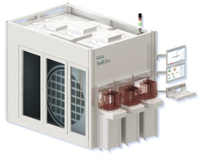
 [ <SemDex A> Fully-Automated System ]
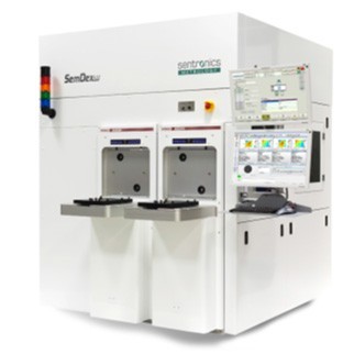
 -