


C&D Semiconductor Services, Inc. (USA)
Products
C&D Semiconductor’s products and services cover wafer handling, processing, and inspection requirements in semiconductor manufacturing.
Applications
SmartPro
P9000 Cluster Processing systems - for Photo resist coat/develop/clean steps for all wafer sizes. Provides thinned wafer handling and processing such as pre-dice protect coat, post-clean and de-bonding steps. Cu Bump Developer for 100um thick dry laminate films.
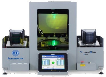
SmartVision
- V1020 - Microscope Loader - Inspection of wafers with automated wafer handling, defect identification and tracking.
- V2000 - Bright Light Inspection - up to 4 different light sources to identify various types of wafer damage - defects, particles, scratches, etc.
- V3000 - Microscope & Bright Light Inspection - combined Bright light inspect with automated microscope loader for quick transfer of defects identified with Bright Light to Microscope Loader for magnified pictures and location details capture.
SmartSort
- S5000 - Wafer sorter for multiple wafer sizes(50mm - 300mm) and multiple wafer cassettes with ID tracking each wafer.
- Dual end-effector for max throughput, cassette mapping, OCR, M12, M13T7, Barcode - with PC based SmartSort GUI.
Mission Statement
We endeavor to be a leader in the semiconductor equipment-manufacturing industry. Toward that end, we strive to provide our customers with innovative, high-value, low-cost, state-of-the-art technology solutions.
-
 [
[Bright Light Inspection System ] -
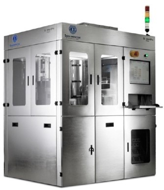 [
[Macro-Scope Defect Review System ]
Website